In the fast-paced world of electronics manufacturing, the margin for error is non-existent. Consumers demand smaller, faster, and more durable devices, forcing original equipment manufacturers (OEMs) to rethink how components are fabricated. At the heart of this hardware evolution lie two critical manufacturing pillars: custom precision stamping E precision finishing for electronics. Together, these processes dictate not just the structural integrity of a device, but also its electrical conductivity, thermal management, and overall lifespan.
Whether you are designing the next breakthrough medical wearable, an advanced automotive control unit, or a high-density server rack, understanding how to leverage these twin manufacturing disciplines is your key to market dominance.
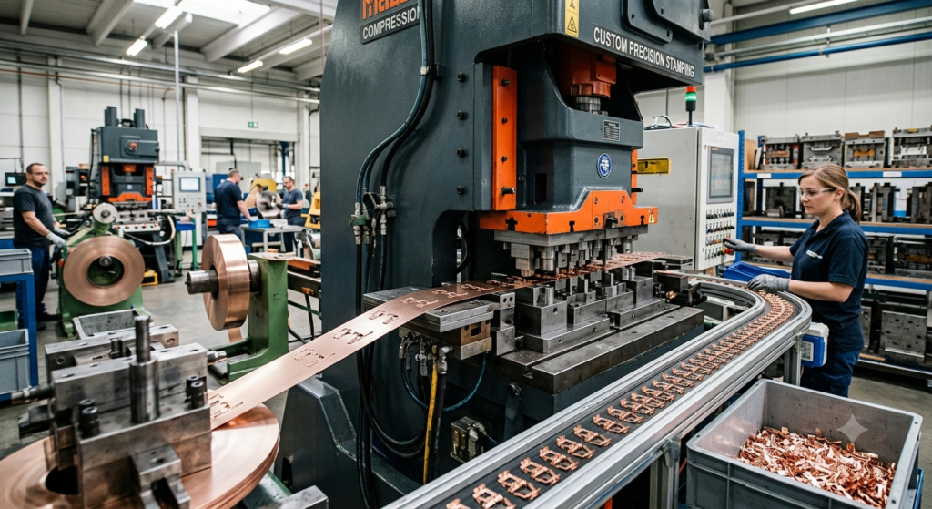
Why Custom Precision Stamping is the Backbone of Modern Electronics
When we talk about high-volume production with microscopic tolerances, standard stamping methods simply won’t cut it. Custom precision stamping is the specialized process of transforming raw metal coils into intricate, highly accurate components using bespoke dies and progressive pressing techniques.
The Micro-Miniaturization Challenge
As PCB layouts shrink, the demand for ultra-thin, complex metal parts skyrockets. Custom stamping allows engineers to create features measuring mere fractions of a millimeter. We are talking about components like:
- Micro-connectors and terminals
- Battery contacts and springs
- EMI/RFI shielding cans
- Lead frames for integrated circuits
Using advanced progressive die stamping, a single strip of metal undergoes multiple operations—cutting, bending, coining, and piercing—at incredibly high speeds. This ensures that the millionth part off the assembly line is identical to the very first, maintaining a level of repeatability that CNC machining simply cannot match at scale.
Pro-Tip for Hardware Engineers: Early supplier involvement (ESI) is crucial. By collaborating with a stamping specialist during your initial design phase, you can optimize part geometry for the stamping process, drastically reducing material waste and die-maintenance costs down the road.
Elevating Performance: Precision Finishing for Electronics
Stamping out a perfect part is only half the battle. Raw metal components are vulnerable to oxidation, environmental wear, and electrical resistance. This is where precision finishing for electronics becomes non-negotiable.
Finishing isn’t just about aesthetics; it is a functional requirement that alters the surface chemistry of the stamped component to meet strict electrical and mechanical specifications.
Essential Finishing Techniques and Their Functions
Different electronic applications require targeted surface treatments. Here are the industry standards that drive modern device reliability:
| Finishing Process | Primary Material Used | Key Benefit for Electronics |
| Gold & Silver Electroplating | Precious Metals | Exceptional electrical conductivity and oxidation resistance; perfect for high-frequency signal contacts. |
| Nickel Plating | Sulfamate or Electroless Nickel | Serves as a robust barrier layer to prevent copper migration and provides excellent wear resistance. |
| Tin Plating (Matte) | Pure Tin | Offers superior solderability for PCB mounting while minimizing the risk of “tin whiskers.” |
| Anodizing | Aluminum Oxide | Provides structural corrosion resistance and electrical insulation for device enclosures and heat sinks. |
Without these precise finishing steps, even the most accurately stamped terminal can fail in the field due to galvanic corrosion or signal degradation. By pairing custom stamping directly with specialized finishing, manufacturers create components that can withstand harsh environments—from the humid depths of industrial factories to the vacuum of aerospace applications.
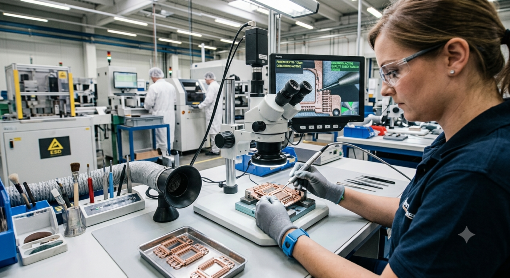
The Synergy: How Integrated Stamping and Finishing Streamline Your Supply Chain
In the electronics supply chain, fragmentation is a major risk factor. If Company A stamps your parts, and Company B plates them, you are looking at increased lead times, shipping costs, and a massive headache regarding quality control accountability.
When you partner with a manufacturer capable of handling both custom precision stamping E precision finishing for electronics under one roof, you unlock significant operational advantages:
1. Seamless Quality Assurance
When a single quality management system oversees both fabrication and surface treatment, the risk of cross-contamination or handling damage drops to near zero. Dimensions are checked before E after plating to guarantee that final tolerances account for the added microscopic thickness of the finish.
2. Optimized Material Selection
Choosing the right substrate (per esempio., phosphor bronze, beryllium copper, or stainless steel) requires a deep understanding of how that material interacts with specific plating chemicals. An integrated team ensures that the mechanical properties required for stamping align perfectly with the chemical properties required for finishing.
3. Reduced Time-to-Market
Eliminating the logistical transit between a stamper and a finisher can shave weeks off your production schedule. In the electronics sector, where market windows open and close in the blink of an eye, this agility is a massive competitive edge.
Looking Ahead: The Future of Electronic Component Manufacturing
As we push deeper into the eras of 5G, IoT, and electric vehicles (EVs), the demands on precision manufacturing will only intensify. High-power EV busbars require heavy-gauge custom stamping paired with specialized selective plating to handle massive electrical currents without overheating. Meanwhile, wearable IoT devices require thinner foils and biocompatible finishes.
The future belongs to manufacturers who treat stamping and finishing not as isolated steps, but as a singular, unified science.
Partner with the Experts
If you are looking to scale your next electronic hardware project, don’t leave your component reliability to chance. Investing in top-tier custom precision stamping and meticulous precision finishing for electronics is the most effective way to guarantee product longevity, reduce field failures, and optimize your manufacturing spend.
What challenges are you currently facing with your electronic component tolerances or plating reliability? Let’s connect and discuss how our integrated engineering team can optimize your next production run.